Disclosure: PCBWay sponsored the PCBs for this project.
The Graveyard Box 🪦
Last year (2024), I started buying up broken Pokemon games on eBay. The idea was simple: find games that didn’t work, get them working again, and sell them back to players.
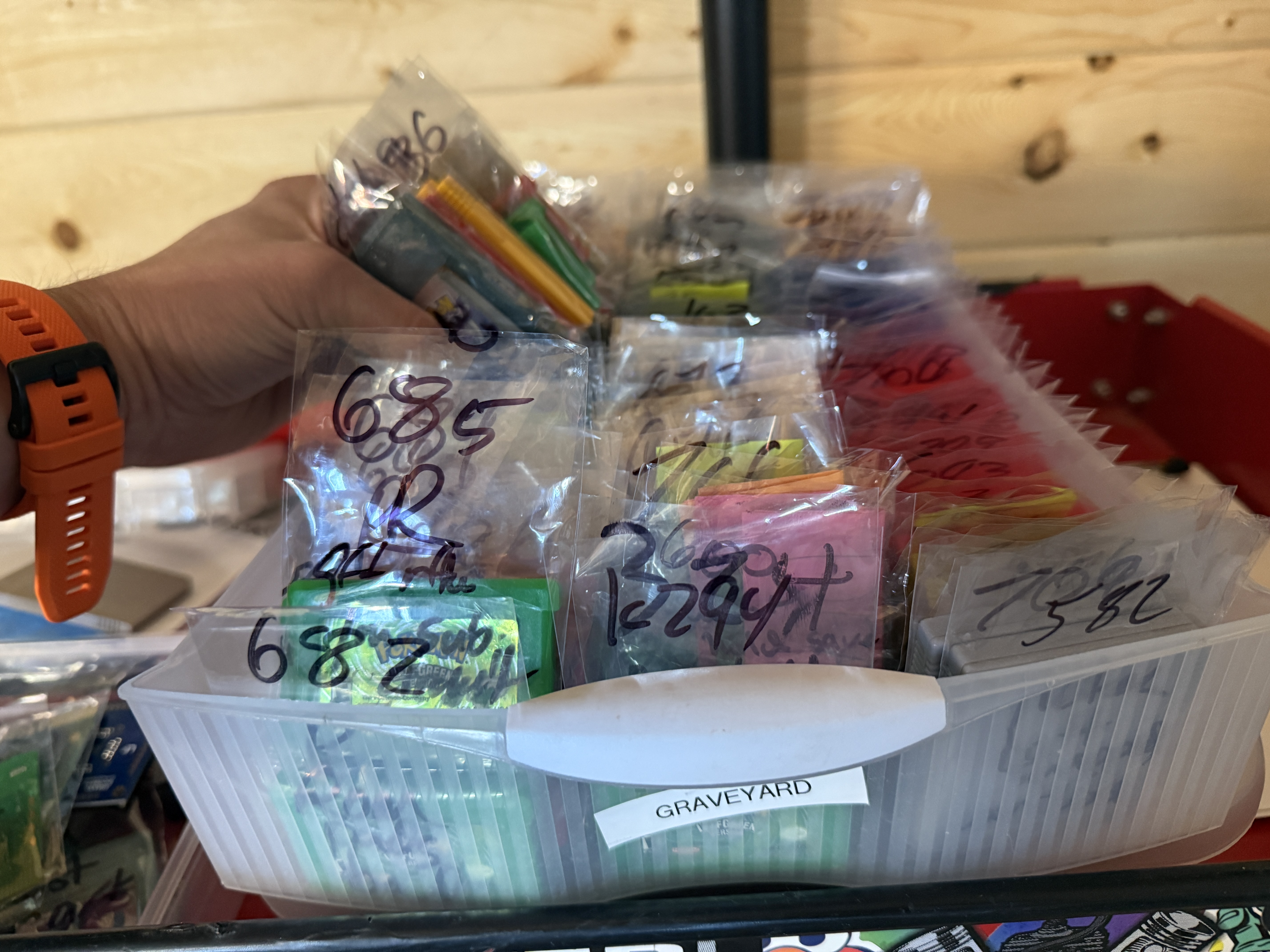
The graveyard box of unfixable cartridges
I learned some basic repair techniques, but ended up with 114 cartridges that I couldn’t fix.
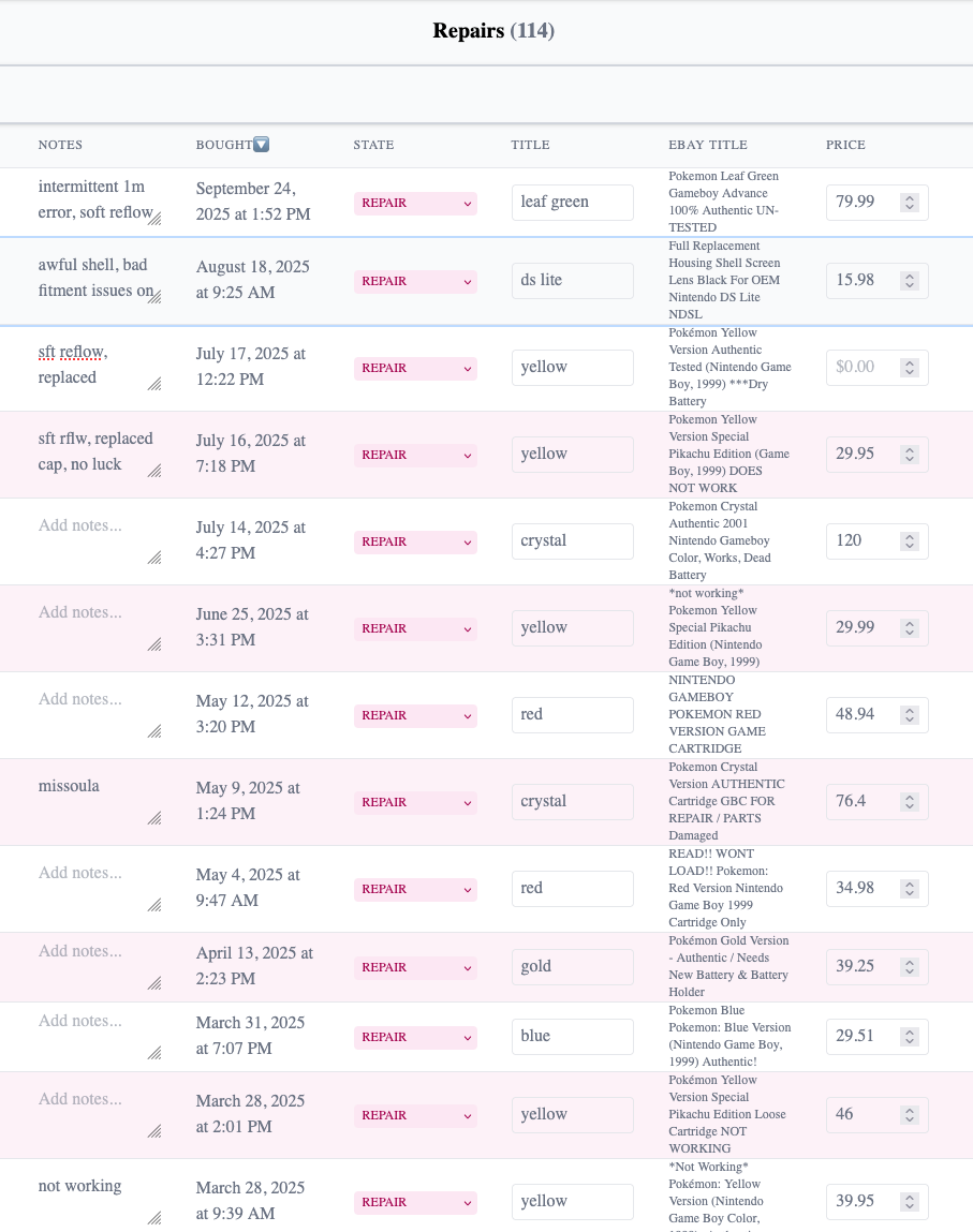
My repair tracking page, broken cartridges ain’t cheap
I’ve spent 5-20 minutes troubleshooting each one. These games still won’t work.
How to Fix a Pokemon Game (Usually)
Most broken Pokemon cartridges fall into a few categories:
Simple cleaning - Isopropyl alcohol and a foam-tip brush work wonders on dust, dog hair, and all kinds of unspeakable gunk found in video games
Reflowing solder joints - Aging solder cracks and breaks connections (sometimes microscopic fractures) and needs to be reflowed. Pokemon Yellow is especially suspect to this for some reason…
Battery replacement - These CR2032/1616 batteries are pushing 25 years old. All need replacing at this point
Bad components - Less common, but capacitors and (much less commonly) resistors do fail. The legs on RAM/ROM ICs can corrode, or be cooked from previous repairs
Trace repair - Corroded battery pads, or damage to the PCB traces. But enamel wire and UV solder mask can bridge broken traces and bring a dead cartridge back to life
The Big Problem: Time ⏰
After trying the easy stuff, you’re left with two time-consuming options:
Option 1: Are the Traces Broken?
Get out your multimeter and start manually probing every trace on the board. On a complex cartridge, this means checking continuity on 60+ pins. For a $5 margin on an eBay cartridge, this is absurd.
Additionally, each cartridge schematic is different, so memorizing all the combinations of test points is difficult. I can easily spend 30min hunting traces on a cartridge.
Option 2: Are the Components Cooked?
Want to know if the RAM or ROM chip is bad? You’ll need to remove it with a hot air station. This is:
- Risky (easy to cook other components, easy to cook the component you’re removing)
- Messy (hot air + flux = sticky mess)
- Time consuming (remove the component, solder it to a known good board)
My graveyard box exists because these diagnostic techniques are risky, and take a ton of time to run through.
But what if I could quickly test all traces automatically? That would eliminate one option and save me time…
Failed Attempts ❌
I tried a few approaches before landing on the bed of nails solution.
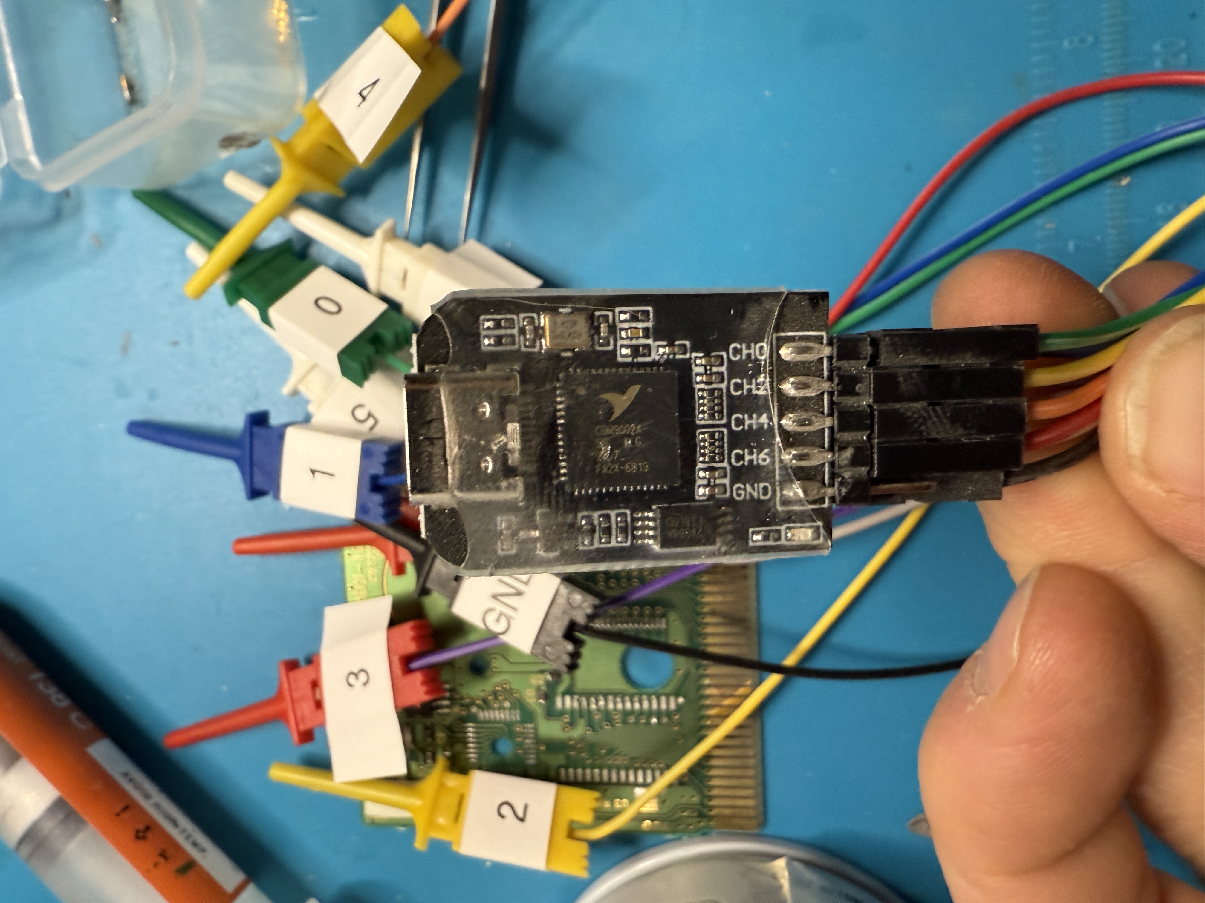
Data Recovery Needles
Forensic hard drive probe needles from AliExpress
These looked promising: they’re used to probe SD cards / SSDs that have been destroyed. Each needle is individually adjustable and can be lined up with all the test points on the Gameboy cartridge, and then measured for continuity to find broken traces.
But swapping cartridges would mean carefully removing and repositioning dozens of probes each time. There’s also not enough needles for the 60+ test points. I gave up on this idea pretty quickly.
Logic Analyzers
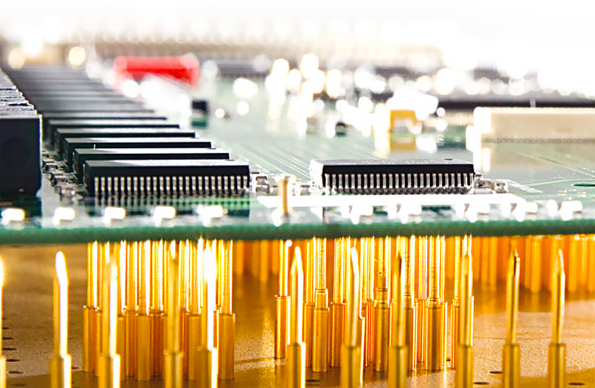
What if I analyzed each of the digital signals from the 32 connector pins?
The 32 gold plated connector pins on Fire Red
Then I could graph what a working Gameboy cartridge looks like, and compare that graph to a broken cartridge to see which pins aren’t firing.
I tried doing this with a DLA v2.1, which can do 8 channels.
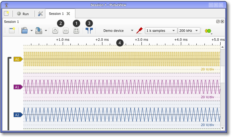
I used PulseView to visualize the output from the DLA
DLA v2.1 - 8 channels isn’t enough
The problems:
- Too many test probes needed (32+ just for the cartridge edge connector)
- Swapping cartridges would be faster than the forensic needles, but still slow
- The legs on each IC can’t be hooked on with test probes: the tolerances are too tight
The solution: do what Nintendo did
Bed of Nails ✨
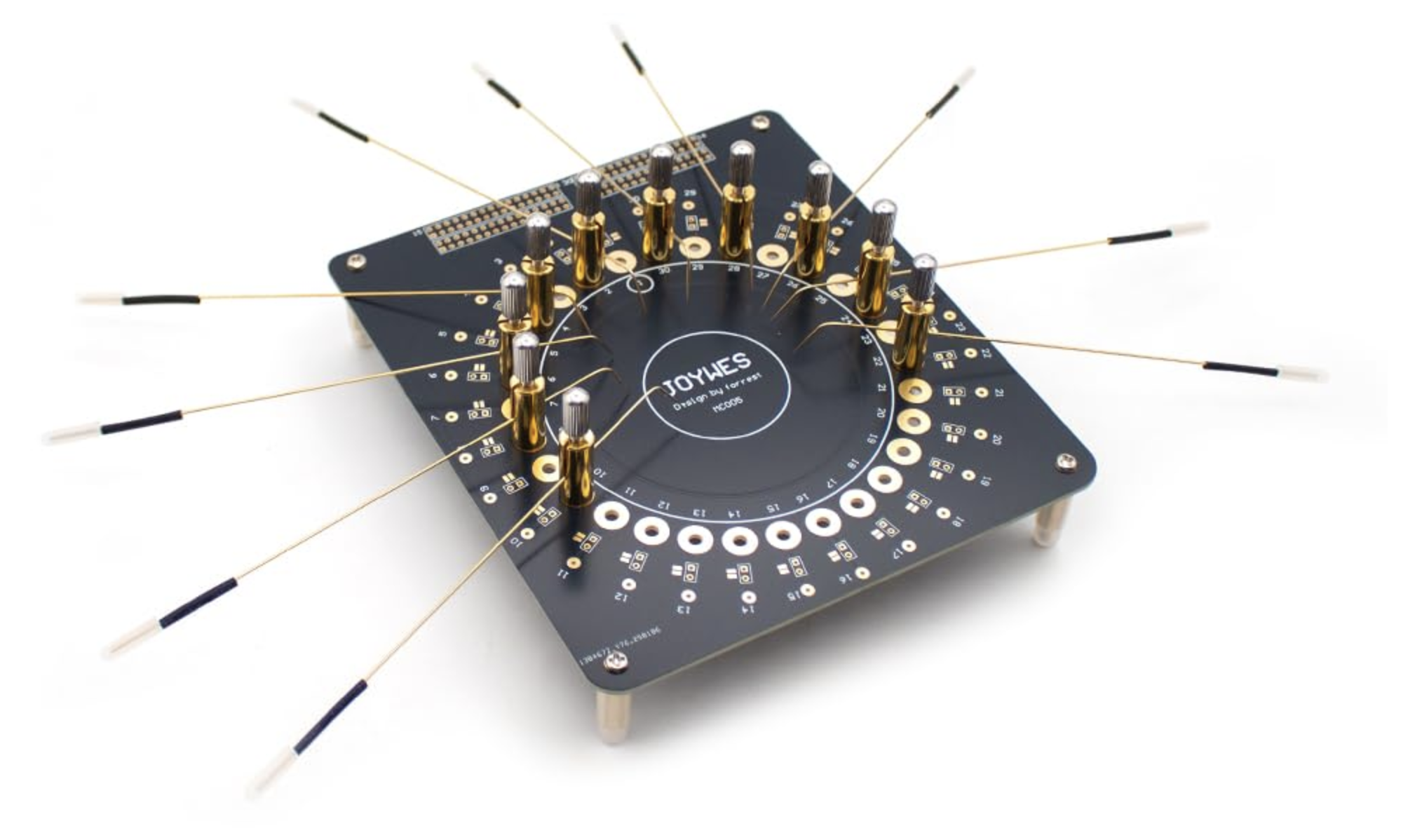
An example bed of nails test fixture
Bed of nails fixtures are common in electronics manufacturing. Spring-loaded pogo pins make contact with test points on a PCB, allowing for quick swapping of PCBs.
Gameboy cartridges are perfect for this approach - they have built-in test points on the PCB that were probably used by Nintendo themselves.
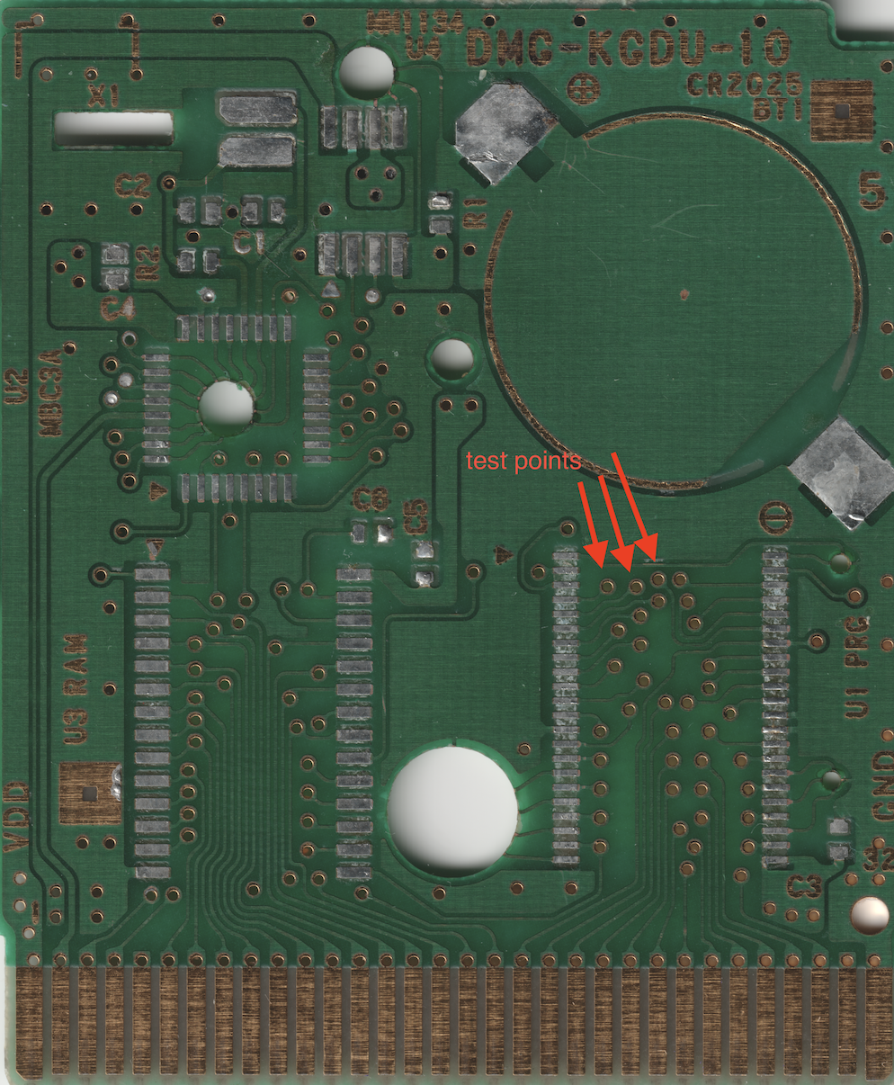
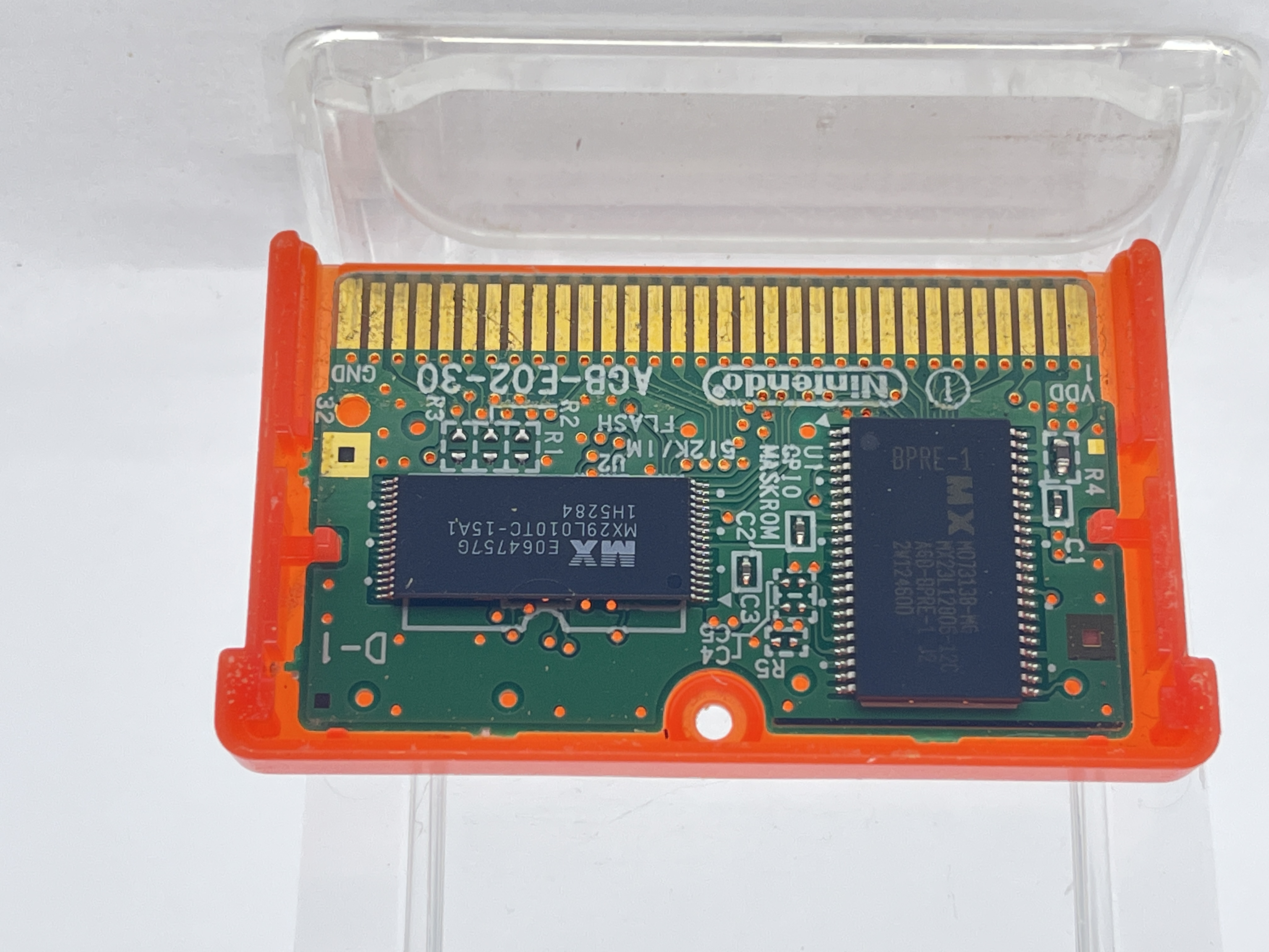
There are dozens of test points underneath components on KGDU
I decided to target specifically the DMG-KGDU-10 board - the PCB used in Pokemon Silver, Gold, and Crystal. If I can fix even one Pokemon Crystal cartridge, the investment pays for itself (these sell for $150-180)
Finding the Right Pogo Pins
Not all pogo pins are created equal. The spacing between test points on a Gameboy cartridge is incredibly tight - standard through-hole pogo pins are too large.
I researched two main options, Mill-Max and Harwin, and Harwin is the only manufacturer with an off-the-shelf pogo pin with a <1.2mm pad footprint.
The catch? They’re expensive. $0.71 per pin, and I need ~60. 💸
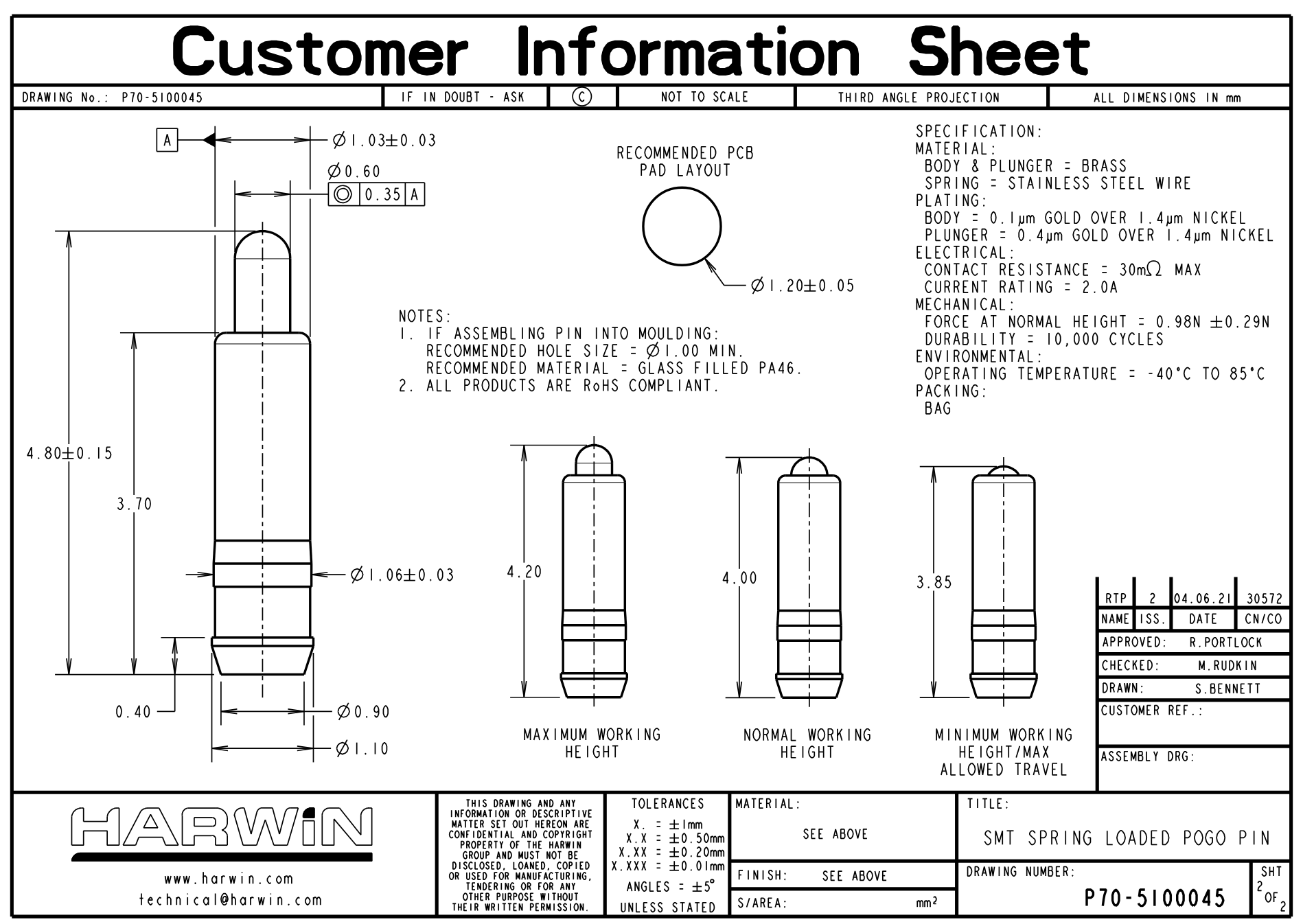
The Harwin P70-510 Spring Connector
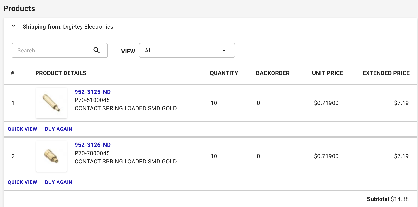
DigiKey prices for pogo pins
Designing the Test PCB
My goals for the first prototype:
- Prove pogo pins work (spring / actuation)
- Prove pogo pin footprints work inside the highly congested areas
- Prove that I can align the pins with the test points on the DMG-KGDU-10 board
- Make reliable contact with the DMG-KGDU-10 board, not be jank
Putting the Pogo Pins in the Right Spot
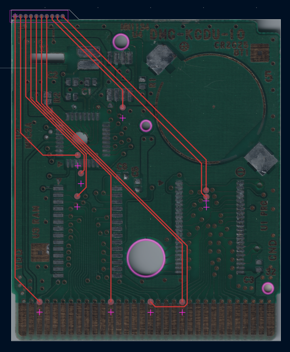
Thankfully, the retro gaming community is incredible and already has high-resolution PCB scans of the DMG-KGDU-10 board (link).
The process:
- Import the PCB scan
- Align test pad locations to the scan
- Place pogo pin footprints
- Route to edge connectors for testing
- Add mounting holes for a test fixture
Reference Images
How do you know where to put the pogo pins so it aligns with the Gameboy cartridge’s test points?
I imported the DMG-KGDU PCB scan as a reference image and locked it to the User.1 layer: this prevents me from dragging the image around accidentally as I shuffled pins / routes, and User.1 layer is used for annotations / references that aren’t exported.
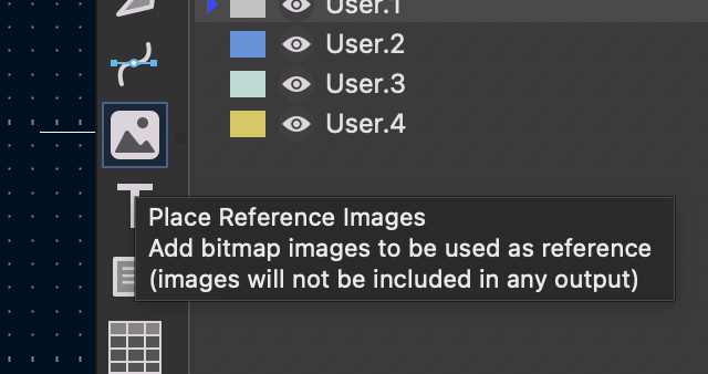
Add reference image on the toolbar
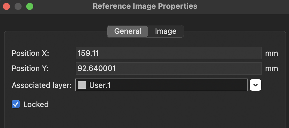
Setting the reference image to ‘locked’ in the User.1 layer
Putting It Together
The first test board uses a few traces to prove pogo pins can be placed in congested areas, and spread out enough that any misalignment or scaling issues should be obvious.
The test board layout
Ordering from PCBWay
Although PCBWay sponsored this project, I was already planning to use their PCB service. I’ve had amazing results with complex PCB cutouts before, like the Datadog PCB they manufactured:
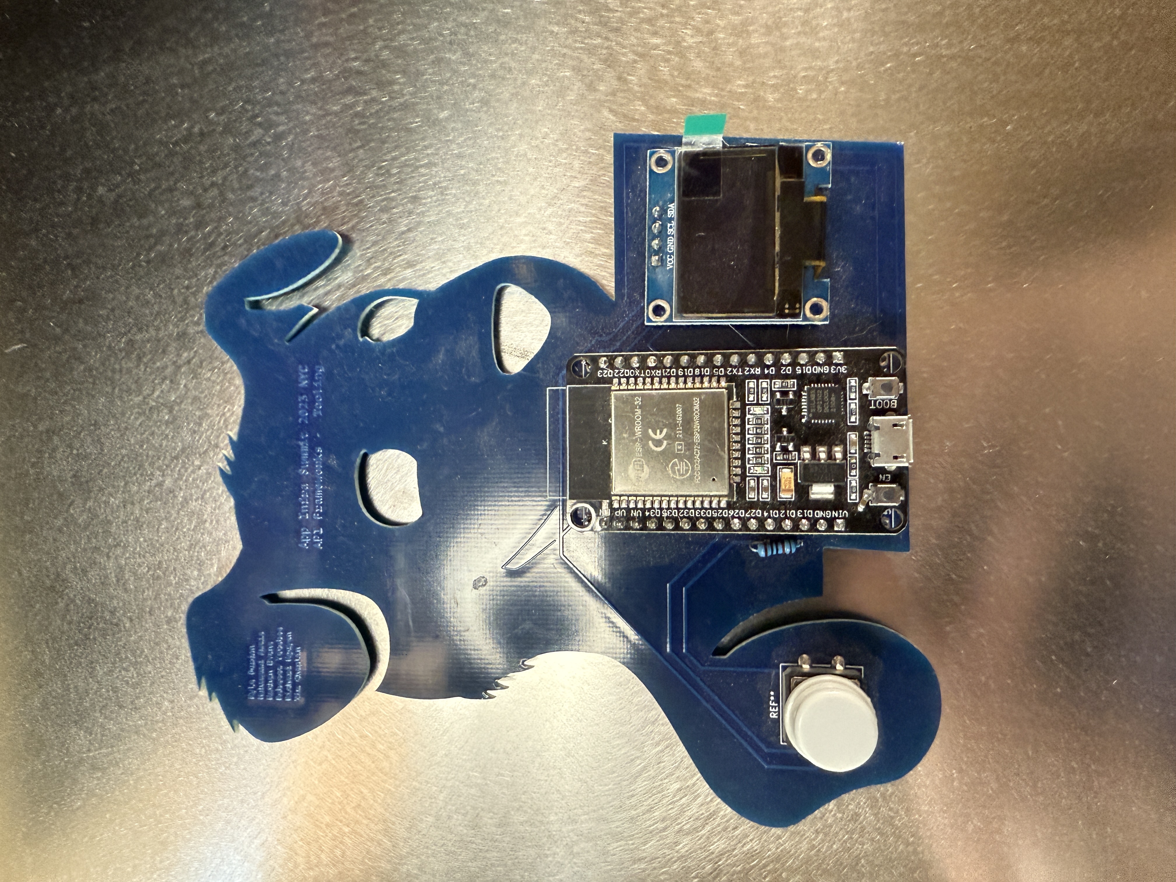
An ESP32-powered clock of ‘Bits’, the Datadog mascot
Like previous PCBWay orders, the process was straightforward:
- 5 boards + 1 SMD stencil: $74.80
- Ordered August 25th, arrived September 12th (18 days)
PCBWay has a Kicad plugin that makes the export of project files easy: when you’re satisfied with the design, install the plugin, and export directly.
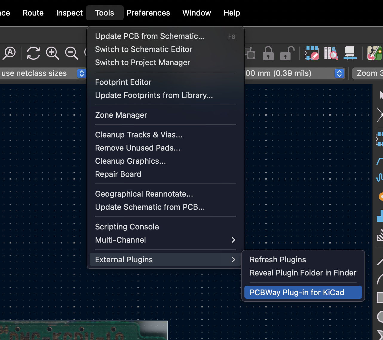
PCBWay plugin for KiCad
My favorite part about using PCBWay is a support engineer will verify your PCB design before it’s shipped to production. For example, I didn’t have any thru-holes because the pogo-pins are SMD mounted, and this raised a flag.
As a hobbyist, I really appreciate the human review keeping me from doing something stupid or messing something up with the exported file.
PCBWay double-checking that SMD pads were intentional
The PCBs
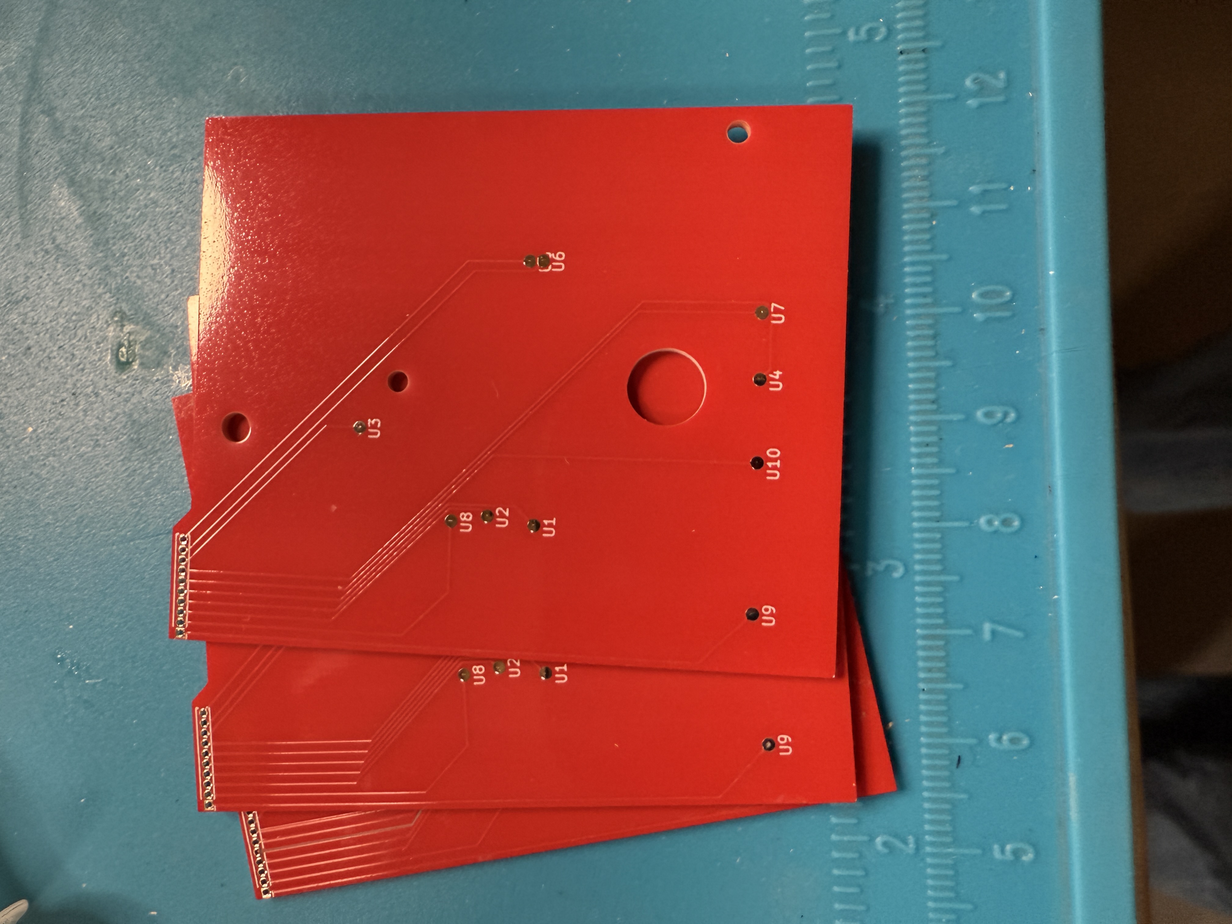
Fresh PCBs…
I was impressed with the PCB quality. Even the highly congested areas (e.g. U6) were printed with space between pads, and no collisions. Precision stuff!
Assembly Challenges
Hot air station: Complete failure. The pogo pins fly around, don’t stand up straight, and generally refuse to cooperate. This might be a skill issue, but I couldn’t make it work.
Mini hot plate: Better results.
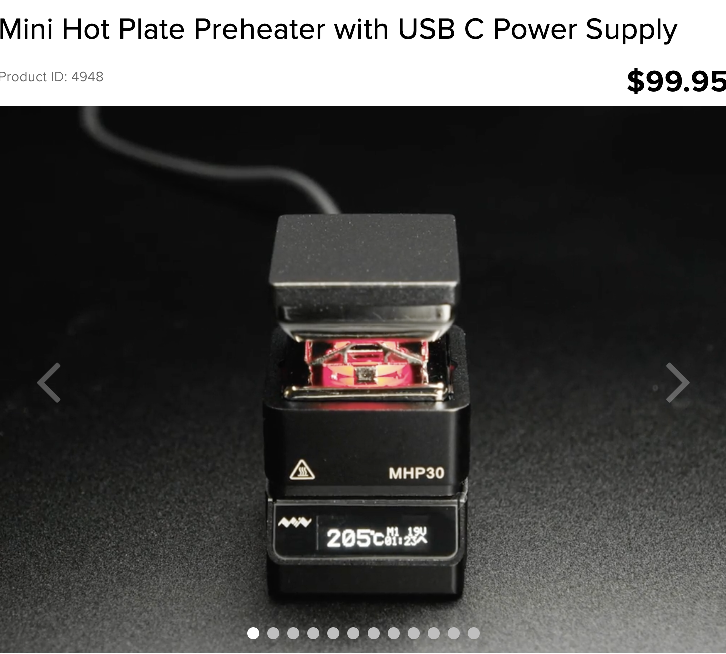
This thing is great for reflowing a section of a PCB, I love mine
The mini plate improves on the hot air because the pins aren’t flying away, but alignment is still tricky.
The PCB soaks up a lot of the heat from the mini plate, which isn’t a big deal for big components: they have enough mass to stay in place as the board cools. But for little pogo pins, it’s easy to bump the PCB and the pins go flying out of alignment because the PCB is still hot.
Hand soldering: The winner. Carefully soldering each pin by hand and forcing it flush with the PCB produces the best results.
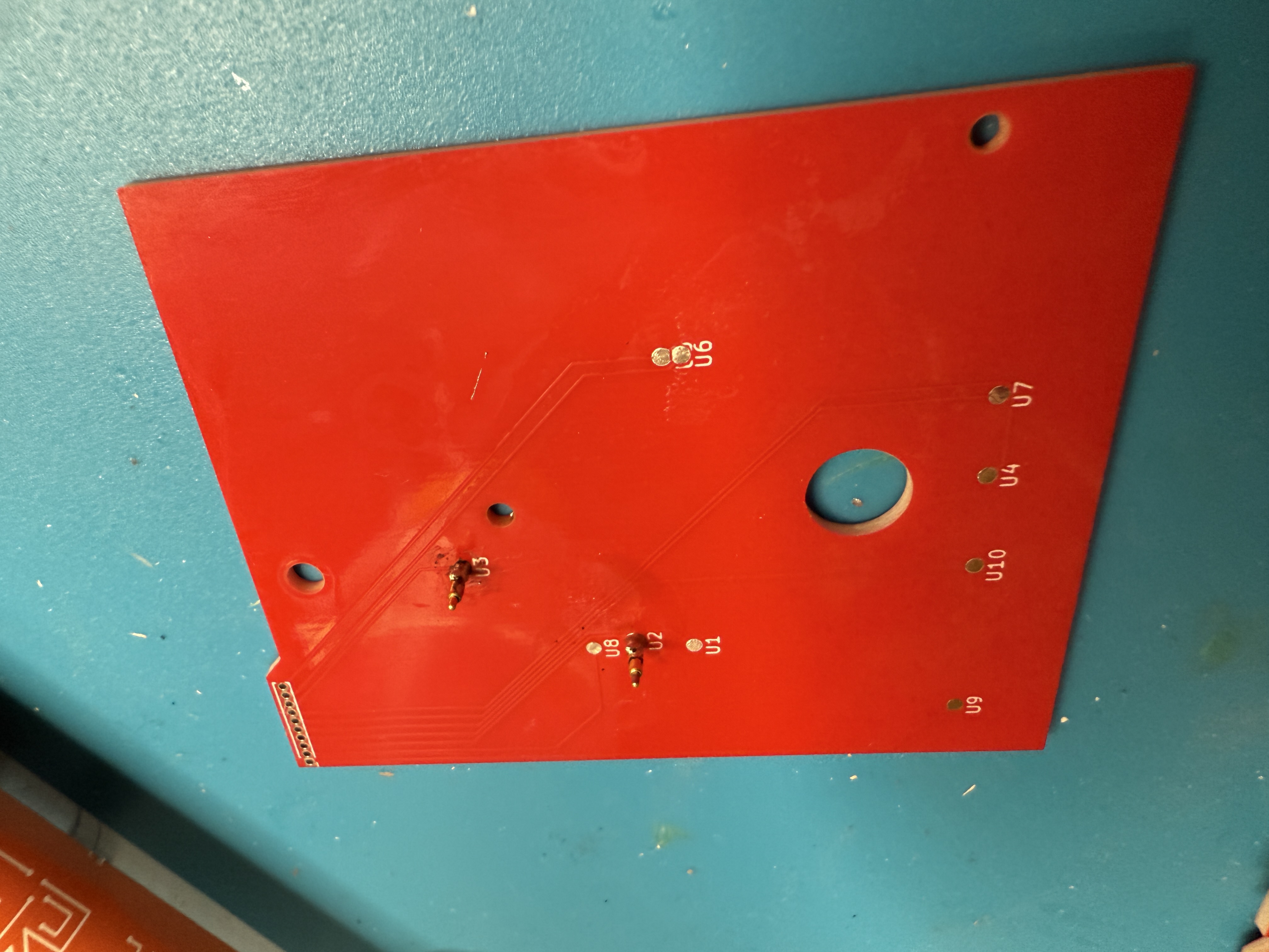
Hand-soldered pogo pins - tedious but effective
I only hand soldered two pins as I lost several in the earlier attempts, and only ordered 10 😳
Success ✅
Turn sound up to hear a continuity beep!
Does It Make Sense? 💰
Pogo pins: $0.71 per pin
- 32 pins for the cartridge edge connector
- 32+ pins for the first layer of test points
- Additional pins for branching test points
- Total: Easily $45-60 in pogo pins per fixture
PCBs: $74.80 for 5 boards + stencil (from PCBWay)
Total investment: ~$120-135 for a working test fixture
Beyond the economics, I’ve had a lot of fun working on this. Understanding PCB design, SMD assembly, and test fixture engineering is fun.
There might be a market for selling these boards as repair tools, which would be cool.
Next Steps 🚀
This first prototype proves the concept, next up is a full test board.
-
Complete coverage - This prototype only covers a few test points. The next version will cover all the test points on DMG-KGDU-10.
-
Automated testing - Right now this requires manual multimeter probing on the header pins. This can be automated with an Arduino, or even a simple multiplexer with LEDs!
-
Support for other boards - The DMG-KGDU-10 is just one board revision. I will slowly expand to the other Gameboy cartridge revisions as I tune the design.
Conclusion
Building a custom test fixture for Gameboy cartridges taught me way more about PCB design and manufacturing than I expected. KiCad reference images, SMD pogo pin assembly, bed of nails testing - all of this was new to me, but I feel like this first PCB proves that a full board is possible.
The graveyard box is still full, but now I have a plan on how to chase down stubborn broken traces without spending 30 minutes probing test points with a multimeter.
Thanks for reading, and thanks PCBWay for sponsoring the boards! Stay tuned for the results of the full board!